
www.industryemea.com
10
'19
Written on Modified on
Ensuring semiconductor quality by getting up close
In the electronics and semiconductor industry, the trend over many decades has been to miniaturise components to satisfy the ever-increasing demand for wearable and mobile devices that have far more processing power than many desktop computers.
In the 21st century, miniaturisation enables a myriad of tiny yet functionality-packed integrated circuits (ICs) to be inserted on to a single PCB. However, one of the issues of working in these miniscule sizes has been the difficulty of research and development professionals checking prior to mass production whether on-board components meet the stringent quality requirements that ensure they will operate reliably and repetitively throughout the life of the device.
When working at such sizes, it’s possible for crucial defects to be invisible to R&D staff who carry out checks using traditional optical systems. Factors that could be missed include defects in the resist film or on a wafer’s edge, lack of uniformity in solder ball bonding used to connect flip chips, poor contacts in wire bonds and much more.
Clearly, the only way of looking so closely at such components to ensure they satisfy standards is through microscopy. However, when working with semiconductors it is important to obtain the most accurate measurements, to have access to pristine, fully detailed images, to be able to identify precisely what the problem is and to be able to communicate findings in an easily understandable format.
One significant issue for many R&D professionals working in this sector is that existing microscopes tend not to possess the depth of field required to generate the extremely clear image that they require. Also, microscopes will often need to be connected to a separate camera and to external software in order to process the images and communicate the results. In addition, R&D staff usually have to carry out preparation work before using several different microscopes – a 2D measurement microscope, a scanning electron microscope (SEM) and others. This preparation can be hugely time consuming and switching between microscopes can present logistical problems if the various microscopes are used by different teams in separate rooms.
The solution
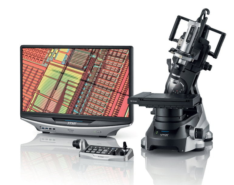
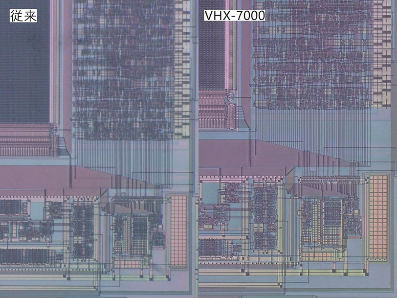
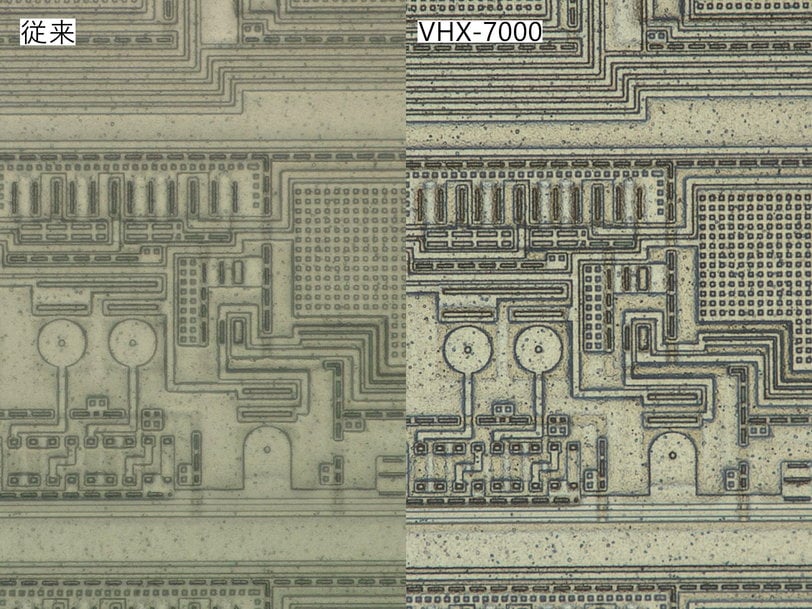
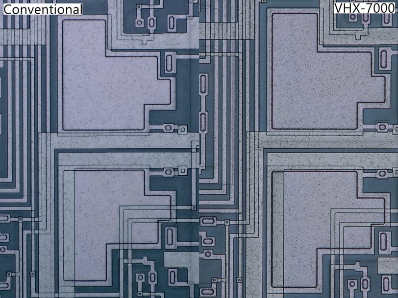
Transforming the way that R&D inspection work is carried out on semiconductors is the world’s first 4K ultra-high accuracy microscope from Keyence. The VHX-7000 digital microscope can provide a new means of inspecting samples and deliver greater convenience to view, capture and measure. This means its images can rival those of an SEM – especially when the optical shadow effect mode feature is enabled.
Although the VHX-7000 is incredibly powerful – it delivers the highest definition in the history of microscopes and offers a depth-of-field 20 times higher than conventional optical microscopes – ease of use is built-in with a simple user interface, sub-menus and step-by-step guide. This means even a novice could capture the highest resolution IC images. Another key feature is the 1TB hard drive that is also integral to the microscope (which is based around a Windows 10 PC) and enables images to be saved on the device and shared over a network or via a USB drive. Detailed reports can also be produced automatically in Excel format for instant sharing with colleagues.
The all-in-one VHX-7000 obviates the need to buy several different microscopes and is highly cost-effective when compared to an SEM. Also, the unit can be upgraded and customised, representing an investment in the future. Different stages, stands and optional features such as the motorisation of axes and a range of optical lenses can be added to the base model depending on the user’s requirements.
As the only 4K digital microscope in the world, the VHX-7000 is particularly suited to the semiconductor market and surpasses traditional lens-based microscopes that rely on eyepieces. As well as its superior magnification of minute features (from 20x to 6000x), the Keyence unit has the ability to subtly shift the finely-tuned XY motorised stage automatically to increase resolution by 33%. The ‘stitching’ of several individual images function has been simplified due to the powerful on-board software with intelligent algorithms that are capable of evening out lighting and diffusing it over the inspected part.
The future
Says Claire Lillywhite, Applications Engineer, Metrology & Microscopy Divisions at Keyence: “Whether looking to do checks on wafer bonding and packaging or carry out non-destructive final testing or a range of other R&D inspections, the semiconductor industry now has a solution to the many issues that have bedevilled it in the past.”
To get more information: www.keyence.co.uk/semicon19
To Find Other Keyence paroducts, visit our website...www.keyence.co.uk
