
www.industryemea.com
16
'23
Written on Modified on
180NM PROCESS FAMILY NOW ONLINE AT AMS OSRAM WAFER FAB IN CENTRAL EUROPE
Benefit from the Full-Service-Foundry’s high-performance speciality analog and mixed-signal 180nm process to create your next-generation sensors, sensor interfaces and emitters.
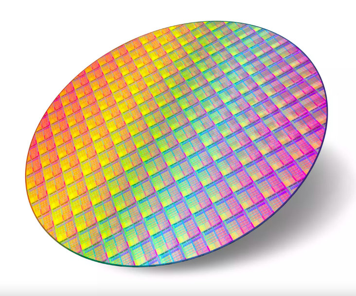
The new C18 180nm CMOS speciality technology, which will be manufactured in ams OSRAM’s 200mm fabrication facility in Austria, is ideally suited for sensors and sensor interface devices in an ever-growing variety of applications – in industrial, medical, and automotive, as well as consumer markets. The process will also be qualified for automotive or medical applications. Designs can begin immediately. Volume production release on C18 180nm technology is scheduled for the upcoming quarter. This is based on industry-standard technology from one of the world's leading semiconductor contract manufacturers, ensuring second-source capability with 100% electrical compatibility.
A high-performance process for analog and mixed-signal devices
The introduction of the C18 180nm CMOS process technology offers customers additional analog and mixed-signal device manufacturing options:
- Low-leakage/high-density digital library
- Extended analog wafer acceptance data (WAT) parameters
- Extensive set of high-quality devices:
- 1.8V/3.3V with 1.8V/5.0V planned for introduction
- Dual-gate oxide and triple-well options
- From three to six metal layers
- Native, isolated CMOS transistors
- NPN and PNP bipolar transistors
- Single MIM (2fF/µm2)
- Several resistor types: poly, 1k high-resolution poly, precision poly
- One-time-programmable (OTP) memory
The process also supports advanced ams OSRAM production technologies such as optical coating – which may be used to implement on-wafer optical filters – and through-silicon vias (TSVs) for optimized routing of sensitive or critical signals. We aim to make the process easy and seamless. The C18 180nm CMOS process is backed by a rich set of tools, resources and services. Our Process Development Kit (PDK) provides chip designers with a plug-and-play toolset for C18 implementations. It offers improved analog and mixed-signal features and device performance as well as highly accurate simulation models. Crucially, it facilitates the development of right-first-time designs, helping customers to deliver fast with ever shorter product development schedules.
Design productivity is enhanced by the latest version of the hitkit design environment. This comes with 1.8V and 3.3V NMOS and PMOS devices (substrate based, floating, low-leakage and high-threshold voltage options) and fully characterized passives including various capacitors. Area-optimized high-density and low-power digital libraries support gate densities up to 125k gates/mm2.
Updated digital and analog I/O libraries with up to six metal layers as well as ESD protection cells rated for up to 4kV (human body model) are included. A memory generation service for RAMs and ROMs, as well as zero-mask-level-adder EEPROM IP blocks, complete the offering.
Multiple ways to take advantage of C18
The C18 180nm CMOS process technology in place in ams OSRAM’s Austrian fab/manufacturing facility is available to all customers and will be used for different products, ranging from customer designs produced by our foundry service to application-specific products and open-market products. Foundry customers will use the C18 process technology for the fabrication of their advanced device designs, especially for high-performance mixed-signal products.
C18 status
The start of prototyping and production runs on the C18 line is possible at any time. Regular multi-product wafer (MPW) prototyping services on the C18 line will start in November 2023.
In addition to the 1.8V / 3.3 V variant of the process, there will be a 1.8V / 5.0V version released in 2024. A BCD (Bipolar-CMOS-DMOS) based high-voltage version up to 70V will follow thereafter.
Click here for more information.
