
www.industryemea.com
01
'26
Written on Modified on
Web-Based Tool for RF Antenna Integration
KYOCERA AVX releases "Antenna Integrator Studio" to optimize antenna selection and PCB placement workflows.
global.kyocera.com
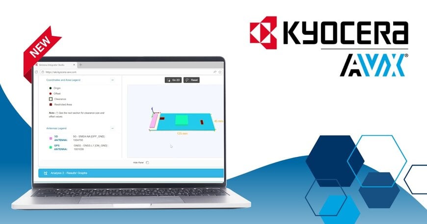
KYOCERA AVX has launched the Antenna Integrator Studio, a web-based engineering platform designed to assist RF design engineers in selecting and positioning embedded antennas. By automating the evaluation of antenna performance based on specific Printed Circuit Board (PCB) parameters, the tool aims to reduce design-cycle bottlenecks, mitigate signal attenuation, and optimize impedance matching for various wireless-enabled devices in sectors such as automotive, IIoT, and medical electronics.
Automated Antenna Selection and Optimization
The platform streamlines the RF design workflow by replacing manual trial-and-error selection with a structured, data-driven process. Engineers input key design parameters, including PCB dimensions, required antenna quantity, and target frequency bands. Users then specify optimization priorities—such as maximizing radiation efficiency or minimizing procurement costs. Upon execution, the tool provides:
- Optimal Positioning: Calculated placement of antennas for the specific PCB layout.
- Performance Analytics: Interactive charts for return loss, peak gain, radiation patterns, and efficiency across defined frequency bands.
- Seamless Integration: Direct download of DXF (2D layout) and 3D CAD files for immediate import into PCB design software.
Workflow and Prototyping
The Antenna Integrator Studio leverages a database containing thousands of simulations for board-mounted embedded antennas. Beyond design analysis, the platform facilitates sample procurement for prototyping. Future iterations of the software are expected to incorporate expanded feature sets and support for additional antenna technologies.
Additional Context: This section details technical specifications not included in the original announcement
In RF design, antenna placement is constrained by the "near-field" interaction between the antenna element and the PCB ground plane. When an antenna is placed too close to the board edge or ground traces, "detuning" occurs, shifting the resonant frequency and significantly increasing the return loss (S11 parameter). Traditional manual design often requires multiple iterations of electromagnetic (EM) simulation or physical prototyping to identify these interactions. The Antenna Integrator Studio likely utilizes pre-calculated EM simulation matrices to model how antenna radiation patterns interact with standard board geometries. By providing exportable CAD files (DXF/3D), the tool ensures that the physical implementation maintains the specific clearances and keep-out zones required to sustain the simulated performance metrics, ultimately preventing common integration failures like impedance mismatch and excessive signal attenuation in battery-constrained IoT hardware.
Edited by Lekshman Ramdas, Induportals editor – adapted by AI.
www.kyocera-avx.com
