
www.industryemea.com
04
'26
Written on Modified on
ALBIS Supports European Polymer Wafer Frames for Semiconductor Manufacturing
Collaboration with Meliori Polymer Engineering develops PPS-based wafer frames manufactured in Europe to strengthen regional semiconductor supply chains.
www.albis.com
Polymer wafer frames for semiconductor manufacturing
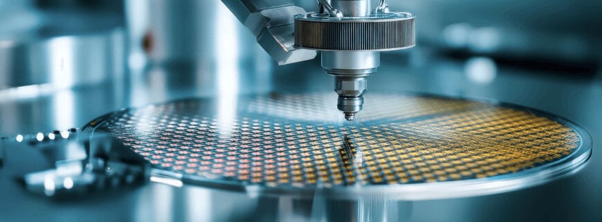
In semiconductor fabrication, microelectronics production, and chip packaging, wafer frames play an essential role in stabilizing semiconductor wafers during processing. These circular frames hold delicate wafers—each containing thousands of integrated circuits—while allowing automated handling by production equipment.
ALBIS is supporting the Croatian startup Meliori Polymer Engineering in the development of polymer wafer frames manufactured in Europe, aimed at reducing dependence on imported components used in semiconductor production. The initiative focuses on creating a European value chain for wafer frame manufacturing, which has traditionally relied on suppliers in Asia.
Strengthening Europe’s semiconductor supply chain
Semiconductor wafers themselves are made of silicon, but the supporting frames used during production are typically manufactured from stainless steel or engineering plastics. These frames ensure mechanical stability and compatibility with automated wafer-handling systems used throughout semiconductor processing.
Meliori Polymer Engineering, founded in 2023 by Croatian engineers Antonia and Marko Omazić, is currently the first European company specializing in polymer solutions for wafer frame production. By producing these components locally, the company aims to support semiconductor manufacturers seeking European-made production components for their fabrication lines.
PPS material solution for precision wafer frames
To meet the mechanical and chemical requirements of semiconductor manufacturing, Meliori collaborated with ALBIS Austria to identify suitable polymer materials. Wafer frames must meet several demanding criteria, including:
- High mechanical rigidity
- Excellent flatness and dimensional stability
- Low surface roughness
- High chemical purity
- Reliable processability in injection molding
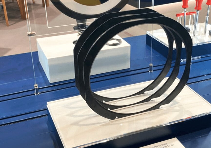
On display at K 2025: The wafer frame for silicone chip production
ALBIS proposed Tedur, a polyphenylene sulfide (PPS) compound produced by MOCOM, as a suitable material for the application. PPS polymers are widely used in electronics and semiconductor equipment because of their thermal stability, chemical resistance, and dimensional accuracy.
The Tedur compound used for the wafer frames is reinforced with mineral and glass fibers, providing the required stiffness and surface quality while maintaining good moldability. Its high flow characteristics also allow processing on smaller injection molding machines, which can be advantageous during early-stage production scaling.
Simulation and material selection support
Beyond material supply, ALBIS provided technical assistance during the development phase. The company performed mold-filling simulations to analyze the flow behavior of different materials during injection molding.
These simulations helped determine the optimal material formulation and processing parameters needed to produce wafer frames with the required dimensional accuracy and surface characteristics.
In addition, ALBIS coordinated further technical validation and quality testing in collaboration with MOCOM. These laboratory tests supported the verification of material performance and contributed to the certification of Meliori’s European production process.
Toward sustainable wafer frame production
The collaboration has also opened opportunities to explore more sustainable material cycles for semiconductor production components.
One concept under evaluation involves the potential use of post-industrial recycled Tedur to create a closed-loop production approach for wafer frames. If technically feasible, such an approach could reduce material waste while maintaining the mechanical and chemical performance required for semiconductor manufacturing environments.
By combining European materials, local production, and technical collaboration, the project aims to contribute to the development of a more resilient semiconductor supply chain within Europe.
www.albis.com
